
Intel continues to share details on future products. This time we will talk about the Xe-HPC Ponte Vecchio graphics accelerator designed for data centers. We have already seen the monstrous GPU of this solution, consisting of 47 individual chips and 100 billion transistors. Now we can see which tiles (as Intel calls the individual GPU chips) are called what.
The main computing unit of such a GPU, like that of Arc gaming video cards, is called the Xe core (Xe-Core). Such a core consists of 8 vectors (512 bits per core) and 8 matrices (4096 bits per core) modules.
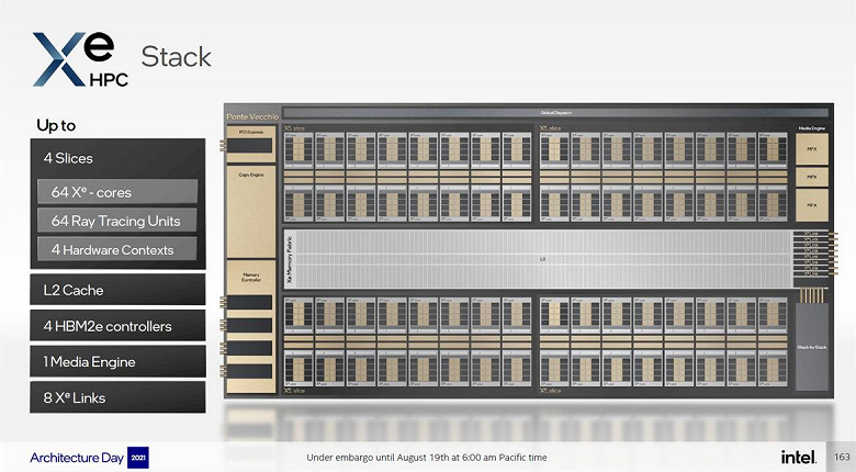
16 Xe-Cores will be combined into a Xe-HPC Slice module. At the same time, unlike the same specialized Nvidia cards, Ponte Vecchio has ray tracing acceleration units. Why they are needed in such a product is not yet clear.
Intel also said that the Ponte Vecchio will be available in two configurations: with one or two stacks. The second option will receive 128 Xe-Core cores and the same number of ray tracing cores. Also, this configuration will receive eight HBM2e memory controllers.
Ponte Vecchio GPUs include five different technology nodes, which can impact both price and availability. Intel also said that the engineering sample with A0 stepping demonstrated a performance of 45 TFLOPS.


0 Comments